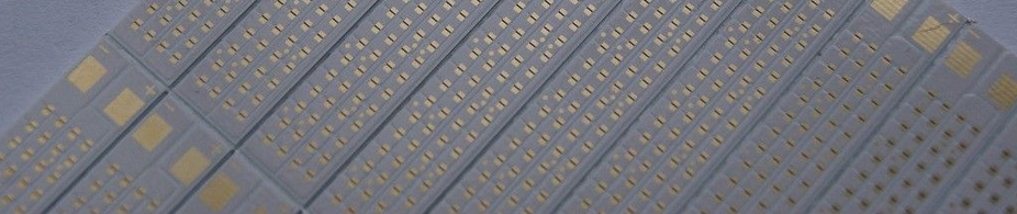


PCB Manufacturing
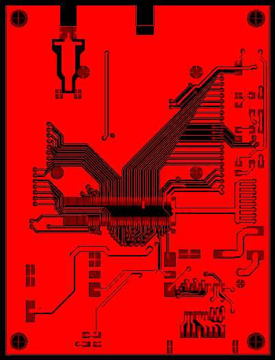
Electronics Solution Group Ltd provides services in designing and manufacturing of printed circuit boards (PCB).
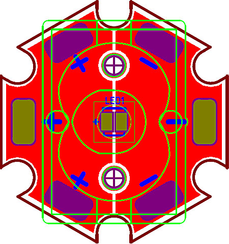
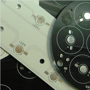
Our designers develop PCB routing in accordance with client`s requirements and specifications. We design single-layer, double-layer and multilayer PCBs (up to 20 layers) with dead or hidden vias; metal core PCBs; flexible and flexibly-rigid PCBs; radio frequencies and super-high frequencies PCBs, etc.
Our staff develop PCBs of any complexity as promptly as practicable. One should e-mail us technical specification to start the ball rolling. After approval for details we start up PCB development in strict accordance with the specifications and SOW.
PCB manufacturing specification:
- Number of layers: 1 - 20;
- Size of the billet (max): 450 mm x 540 mm (up to 600 mm x 1000 mm);
- Stuft: FR1, FR2, FR3, FR4, CEM1, CEM2, Me-base (aluminum, copper, steel, flexible, RF materials;
- PCB thickness: 0.2 mm - 3.0 mm (standard 1.5 mm);
- Minimum dimensions: 10 mm to 10 mm;
- Foil thickness: 9 µm, 18 µm, 35 µm, 70 µm, 105 µm (standard 35 micron);
- Minimum conductor width: 0.2 mm (GOST), 0.1 mm (IPC);
- Minimum clearance between conductors: 0.2 mm (GOST), 0.1 mm (IPC);
- Minimum pad size: 0.4 mm (GOST), 0.2 mm (IPC);
- Minimum plated-through-hole diameter: 0.3 mm (GOST), 0.2 mm (IPC);
- Minimum thickness of inner layer: 0.2 mm (GOST), 0.1 mm (IPC);
- Protective mask covering the surface layer of copper: Hot tinning POS-63 (HASL), immersion gold, immersion silver, flux finishing of copper pads (OSP), ROHS and other (standard HASL coating);
- Colors of mask coating: green, blue, red, black, white (standard: green);
- Silkscreen (text and marks) is available from both sides;
- Color marking coating: white, yellow, black (standard: white);
- Processing: scribing, milling, stamping;
- Electrical testing - manufacture of test prods or "flying probe, adapter" method;
- Packing: simple mica packaging (GOST) or vacuum polyethylene packaging (IPC);
- Turnaround time (typical): 14 days (GOST) (short-term: up to 5 days); from 3-4 weeks (IPC);
We are a provider of all types of PCB in China!